Google Home Headphone Jack
Adding a 3.5mm jack to a Google Home Mini - the hard way
In my living room, I have a pair of reasonably nice speakers (rescued from a skip) connected to an amplifier salvaged out of an old pair of Dell PC speakers. That setup actually sounds pretty good, but doesn’t see much use. It’s a pain to plug something into them: either you plug them into the TV and have to have the TV on, or you plug your phone in and have to keep walking over there.
I bought a cheapy Bluetooth audio module, but predictably the audio quality is dire (continual electrical noise, even with a clean power supply).
Tangentially, my work often sees me at Google HQ in Mountain View, where the Google store is. I’ve been unable to resist the “buy one get one free” deal they had on Google Home Minis on two occasions, meaning I have 4 of the things (always with the intention of hacking - and maybe breaking - at least one of them!) They’re pretty nice devices, and I use them for music a lot.
Now, the Google Home Mini lacks a headphone jack, otherwise my wireless living room audio problem would be solved. How about we fix that?
The Basic Idea
Other people have added headphone sockets to Google Home Minis, generally by just soldering the socket where the speaker is connected. The only thing is, that’s a mono output, and also it’s an amplified signal for driving a speaker, rather than a line-level one for driving another amplifier.
This excellent, detailed teardown gave me an idea: The GHM (Google Home Mini - saves some typing1) uses the TAS5720L, which is a mono digital audio amplifier. What if I could replace this with a different, stereo amplifier? Would it work?
Spoiler: Yes, it does, and the GHM even sends i2s data for two channels. But the channels are the same, so you still don’t get real stereo! 😢
It seemed like a good opportunity to develop my reverse engineering and soldering skills, so I broke out the hot air gun and disassembled a GHM.
Identifying signals
The first thing I wanted to do was to figure out how the GHM was controlling the amplifier. For instance, if it was using the amp’s volume control, or changing the data format setting, then that would be important when trying to replace the amp with something else.
The TAS5720L supports i2s (common digital audio protocol) as well as ‘TDM’ (seems more rare) for the audio input, and has a set of control registers exposed over an i2c bus. So my first step was to try and see what i2c traffic was going on.
I’ve got a cheap 8 channel logic analyser which is compatible with the open source Sigrok signal analysis software and fx2lafw firmware. For <£10 this is a fantastic piece of kit, and I highly recommend everyone to add one to their toolbox. I knew I could use the logic analyser and Pulseview to figure out the i2c traffic, all I needed was some wires.
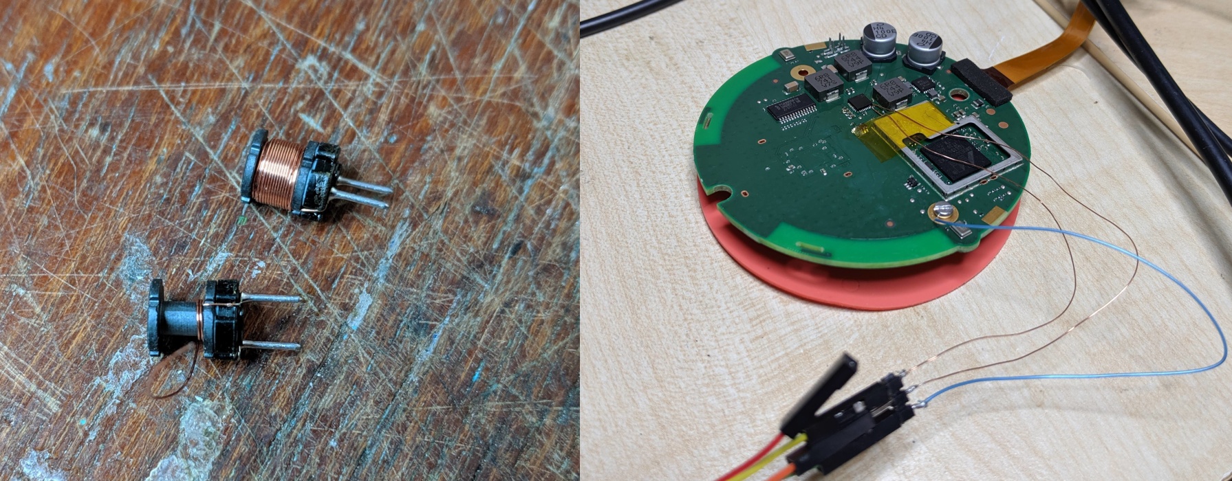
The TAS5720L is a QFN device, which makes it tricky to solder to, though from consulting the datasheet you can see that the i2c pins are positioned around a corner, making them a bit easier to get at. To get some tiny single-core wire, I cannibalised an inductor from my parts drawers.
Soldering on the i2c wires wasn’t too hard, but I had a lot of trouble getting a ground, because the PCB ground plane(s) were absorbing all the heat from my iron. In the end I settled for using a bolt to attach a temporary ground (blue wire).
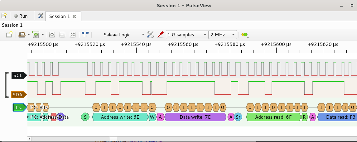
Firing up Pulseview, I could get a trace of all the i2c traffic during bootup (which includes a bootup sound, so the amplifier must be initialised). I was pretty happy to see that my haphazard soldering hadn’t killed the device! All I needed to do was identify which bits were relevant to the amplifier, which has a selectable i2c address.
With sigrok-cli, it’s easy to get a
listing of the traffic in text form, and use grep to pick out which addresses
are being accessed2: (Note the differences between 8-bit addresses in the
screenshot, and 7-bit addresses in the text. That’s always a point of
confusion
when working with i2c, and I apologise for the inconsistency!)
$ sigrok-cli -i bootup_i2c_trace.sr --channels=SCL,SDA -P i2c -A i2c=addr-data | grep "Address write" | sort | uniq
i2c-1: Address write: 17
i2c-1: Address write: 18
i2c-1: Address write: 19
i2c-1: Address write: 37
i2c-1: Address write: 6C
Looking at the traffic and the devices on the board, I identified three active i2c devices:
0x17- LED Controller NXP9956B0x37- Touch Button Controller CY8CMBR31080x6C- Audio amplifier TAS5720L
Address 0x18 is probed, but returns a NAK - perhaps the same software is used
on the full-size Google Home which has more LEDs? Address 0x19 is accessed (and
responds) twice right after power-on, but I never figured out what it is. I’m
interested in 0x6C only.
Using sigrok-cli and sed I grabbed all of the amplifier traffic:
$ sigrok-cli -i bootup_i2c_trace.sr --channels=SCL,SDA -P i2c -A i2c=addr-data | sed -n '/Address \(read\|write\): 6C/,/Stop/p'
i2c-1: Address write: 6C
i2c-1: ACK
i2c-1: Data write: 06
i2c-1: ACK
i2c-1: Data write: 51
i2c-1: ACK
i2c-1: Stop
i2c-1: Address write: 6C
i2c-1: ACK
i2c-1: Data write: 01
i2c-1: ACK
i2c-1: Start repeat
i2c-1: Read
i2c-1: Address read: 6C
i2c-1: ACK
i2c-1: Data read: FD
i2c-1: NACK
i2c-1: Stop
...
Cross-referencing the datasheet, it’s easy to confirm that this data is
correct: the reset value of register 0x01 (Power Control) is 0xFD. I worked
through the trace by hand, and determined that the amplifier is left entirely
in its default state. Importantly, the data format is set to i2s (the default),
the amplifier is left turned “on” all the time, and the digital volume control
is not used. All good news!
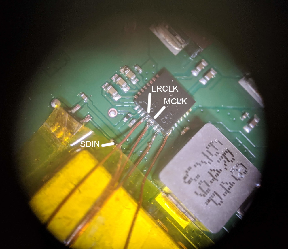
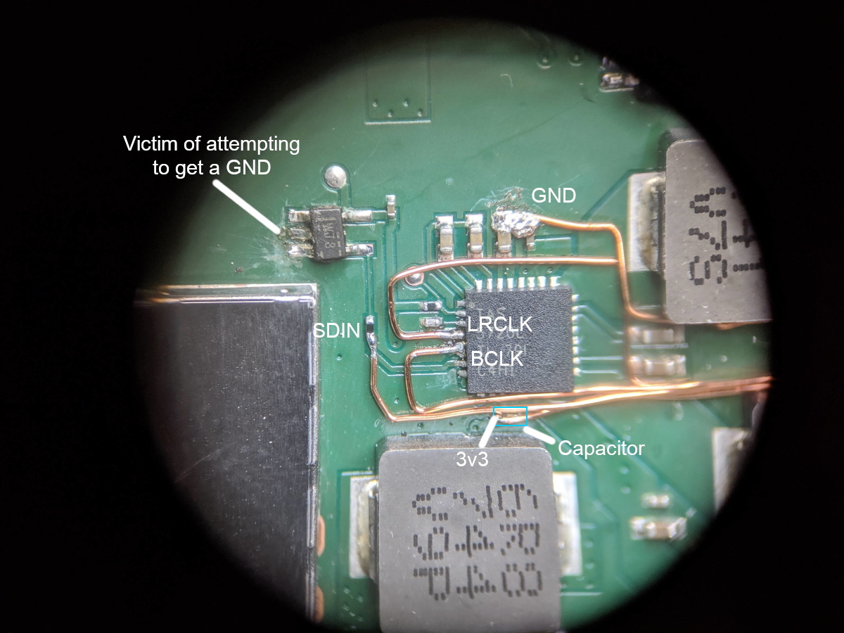
Next was to see if I could get i2s audio, so I soldered on to the audio LRCLK
(left/right clock), MCLK/BCLK (main clock/bit clock) and SDIN (data in)
pins. These were more challenging to solder, as they’re right in the middle of
the side of the QFN. For SDINthere’s a convenient resistor to solder to, but I
didn’t spot anywhere easy to get to the other two signals.
The MCLK and BCLK pins are tied together, and there’s
this note in the datasheet:
If the BCLK to LRCLK ratio is 64, MCLK can be tied directly to BCLK
That will be important for amp selection later.
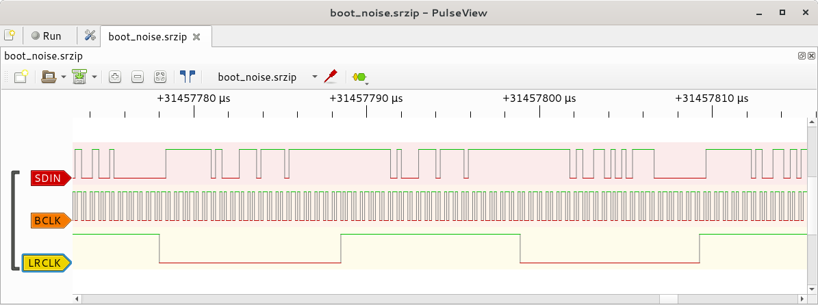
Once again, using Pulseview, I captured the bootup sound. It took me a couple
of tries, because the clock rate was far higher than I anticipated, so I wasn’t
sampling with a high enough frequency. The audio sampling rate looks to be 48
kHz, with 32 bits per sample and two channels, that gives a bit clock rate of
just over 3 MHz!
sigrok can decode various different protocols, and i2s is one of them. I ran
my capture through the i2s protocol decoder, and my machine ran out of RAM and
crashed. So, I extracted a smaller segment and tried again - the RAM usage was
still huge, so perhaps the i2s decoder has a memory leak or something, but I
did manage to get it to export a WAV file:
sigrok-cli -P i2s:sck=BCLK:ws=LRCLK:sd=SDIN -i boot_noise_higfreq.sr -B i2s=wav > out.wav
The audio was very quiet, and for some reason ~half-speed, but it was unmistakably the bootup sound! Using Audacity I could fix up the volume and speed.
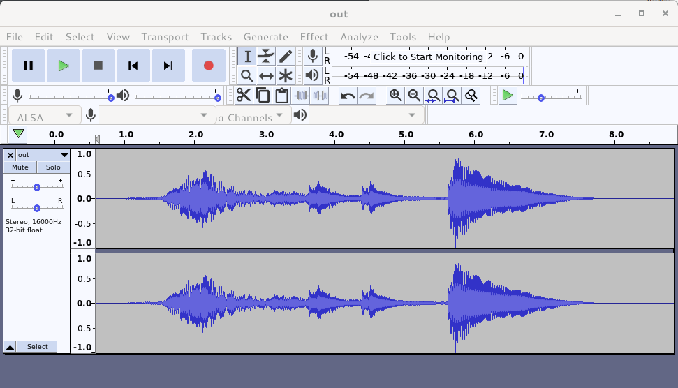
What was great to see, is that the GHM is sending i2s data on both audio channels!
Installing a new amplifier
All that’s left, then, is to get an i2s amplifier and solder it all together.
Little i2s boards are easy to come by, and are often marketed as Raspberry Pi
add-ons. I picked up a pair of
PCM5102A based ones off
eBay. I checked the PCM5102 datasheet
to make sure it could support the combined MCLK/BCLK mode that the GHM was
using - this is supported by shorting the MCLK pin on the PCM5102 to ground
(the PCB has a little solder bridge to do that).
I was planning to use a separate, “clean” 3.3 V supply for the analogue part of the amp, using a linear 3.3V regulator running of the GHM’s 9 V analog voltage rail. I wired it all up:
- i2s
BCLK,LRCLKandSDINas already tested - PCM5102A digital 3.3 V supply from the GHM amp’s 3.3 V digital supply
- PCM5102A analogue 3.3 V supply from an LM1117 3.3 V linear regulator connected to the GHM amp’s 9 V analogue supply
I found that the GHM wouldn’t boot, and it over-current limited the USB hub I was using. Debugging that, I found that the 3.3 V regulator was burning up and it turns out that the PCM5102 board has the analogue and digital 3.3 V supplies connected together. I didn’t spot an obvious way to separate them, so in the end I used the GHM’s digital 3.3 V supply for the whole thing. I hope whatever regulator is supplying that in the GHM doesn’t mind a few extra milliamps!
With that little scare over (the GHM still booted!), the audio still wasn’t
working. After some time prodding around with my multimeter and
oscilloscope, I found that there was a bad solder joint on the LRCLK line on
the board from eBay! I’ve found this to be relatively common if you buy the
absolute cheapest board you can find 😄.
Finally, with that fixed, I had audio out of my newly-wired amplifier.
All righty! Phase 2 complete: i2s amplifier arrived this morning and works (after debugging bad solder from the factory!)
— Brian Starkey (@usedbytes) June 8, 2019
Phase 3: Enclosure and write-up pic.twitter.com/1UQHhaHTKB
Plugging it into the living room speakers, the audio quality was nice and clean, but I discovered that even though the i2s signal has data in both channels, it’s the same data and so I still didn’t have stereo audio, so the whole endeavour is a bit of a waste of time!
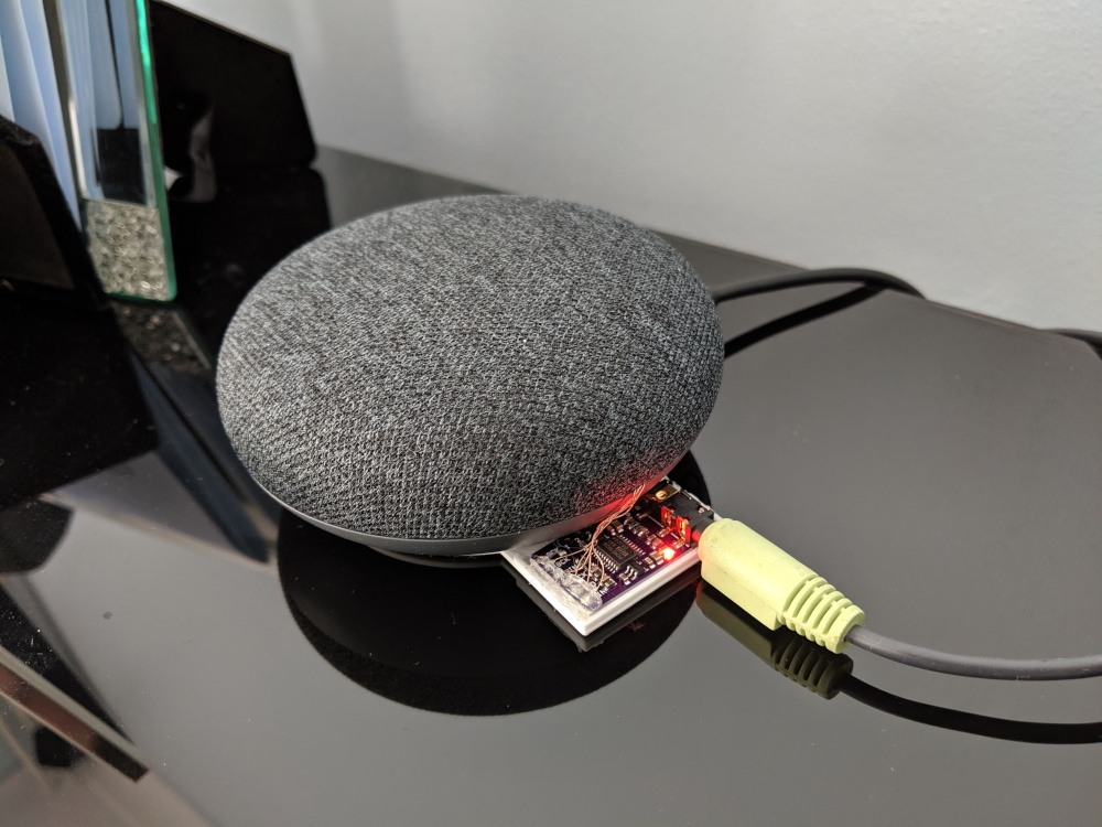
Final wiring and “enclosure”
The last step is to tidy up the wiring and close it all up. I re-did all of my soldering, to get the wires going in the right direction to bring them out of the case. I neglected to take a clear picture of where to get 3.3 V from, but there’s a capacitor in-between the chip and the large inductor - one side is 3.3 V, the other is ground.
As you can see on the teardown, there’s a metal heatsink/audio guide inside the device. I didn’t really want to drill a hole in it, so I routed my wires through the hole where the speaker normally plugs in.
While test-fitting, I found that my tiny wires would fit through the join between the two halves of the case with no modification needed! So I didn’t even need to cut a hole in the plastic. That means this whole project can be done without any permanent modifications to the GHM (depending on whether you consider soldering to the motherboard a permanent modification).
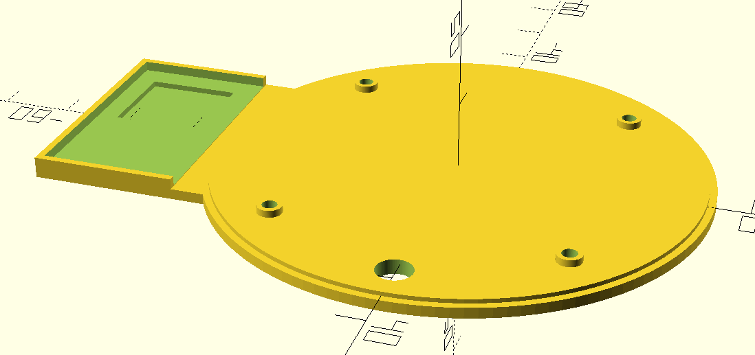
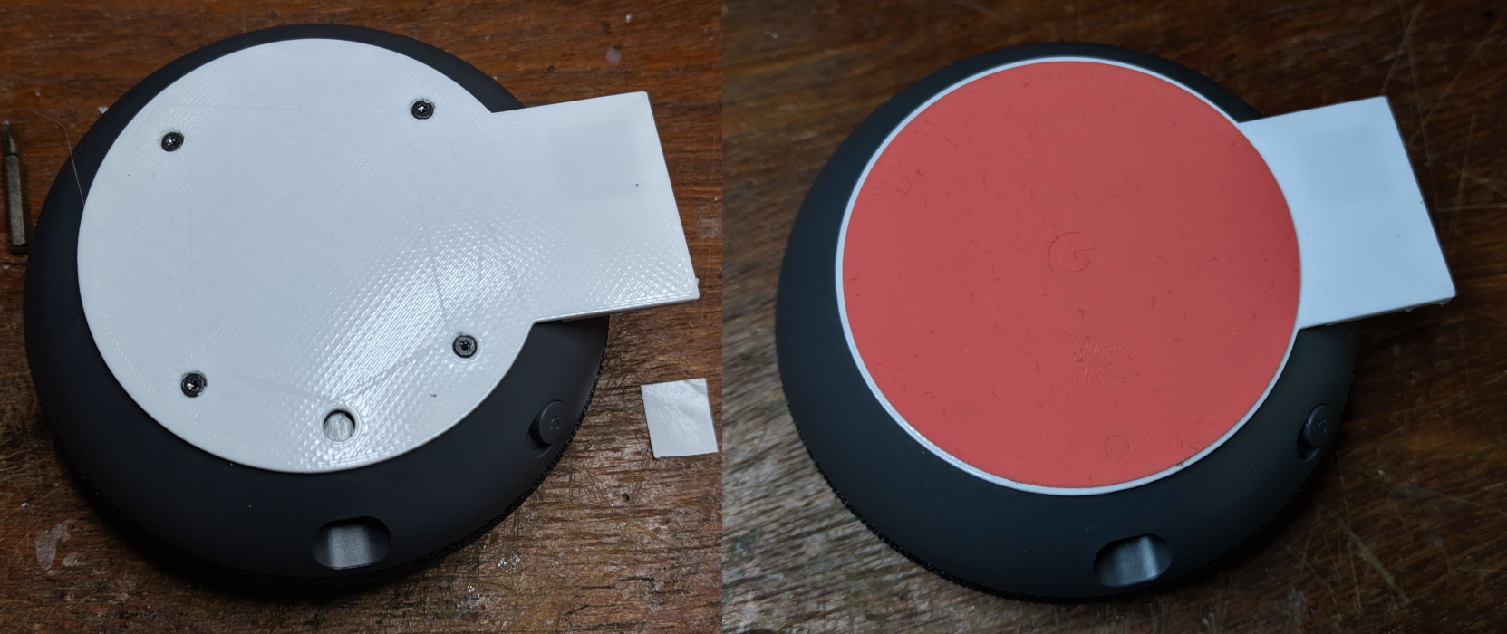
I was planning to 3D print a nice enclosure for the amp, but the shape of the bottom half of the case is a bit hard to model. It seems like some kind of ellipsoid, but figuring out the exact parameters would be tedious. Instead, I just made a plate which bolts onto the bottom, with a holder for the amp PCB. This leaves the amplifier exposed, but does at least hold it securely (with the aid of some hot-glue).
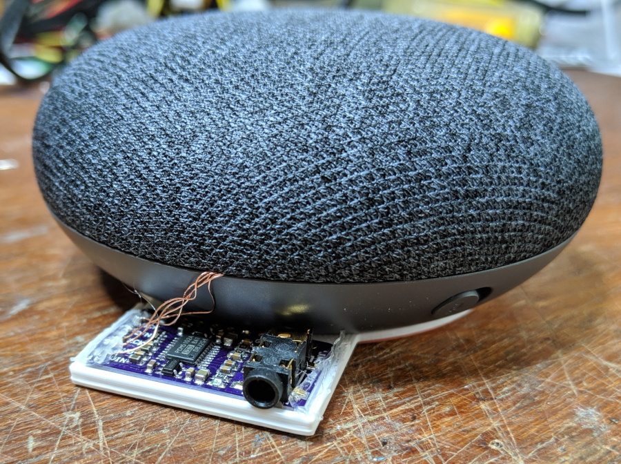
I made the base so that the original screws could go through it, and it fits flush on the base of the GHM. I even stuck back on the rubberised bottom sticker 😄. There’s also a hole, in case I ever need to get to the reset button.
Conclusion
So this whole endeavour was to try and get stereo audio out of the Google Home Mini into my living room speakers. It’s only a moderate success, as the GHM doesn’t output different data on the left and right audio channels.
Still, I’m happy with the result, and it seems like less of a hack than directly wiring in to where the speaker is meant to be.
One interesting thing I’ve noticed, is that they seem to be doing some kind of audio signal processing, probably to compensate for the physical properties of the device. At mid volume levels, the output signal is heavily bass-boosted, and this effect varies with different volume levels. It’s possible that it’s a property of the amplifier I bought, but it seems more likely that Google put some effort in to get the best sound they could out of the tiny device (because out-of-the-box it really does sound good for such a small thing).
Also, the build quality of the whole thing is really really nice. If any of the designers happen to read this, great job on packing everything in and still keeping it glue-free and easy to disassemble/reassemble, with no clips to break or overly fiddly bits!
If you’re crazy enough to want to replicate this project, the STL file for the base is available here.
-
Those guys really need to work on their naming: “Hey Google, play me some music on Google Play Music”, are you serious?! ↩︎
-
If you want to have a play with sigrok yourself, you can download the i2c bootup data capture here ↩︎